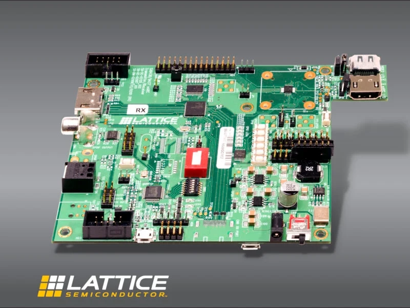
Implementing an HDMI transmission solution on a Lattice FPGA involves using the FPGA's programmable logic and dedicated resources to handle the high-speed data transmission required for HDMI. Lattice FPGAs, such as the ECP5 or CrossLink families, are well-suited for HDMI applications due to their low power consumption, small form factor, and support for high-speed interfaces. Below is a step-by-step guide to implementing an HDMI transmission solution on a Lattice FPGA:
1. Overview of HDMI
HDMI (High-Definition Multimedia Interface) is a widely used standard for transmitting uncompressed video and audio data. Key features include:
- High-Speed Data Transmission: HDMI 1.4 supports up to 10.2 Gbps, while HDMI 2.0 supports up to 18 Gbps.
- TMDS (Transition Minimized Differential Signaling): Used for transmitting video and audio data.
- DDC (Display Data Channel): Used for EDID (Extended Display Identification Data) communication.
- CEC (Consumer Electronics Control): Optional control channel for device control.
2. Lattice FPGA Features for HDMI
Lattice FPGAs offer several features that make them suitable for HDMI applications:
- High-Speed I/O: Supports TMDS signaling for HDMI.
- SERDES (Serializer/Deserializer): Used for high-speed data transmission.
- Programmable Logic: Flexible logic resources for implementing HDMI protocols.
- Low Power Consumption: Ideal for portable and embedded applications.
3. HDMI Transmission Solution Components
To implement HDMI transmission on a Lattice FPGA, the following components are required:
3.1. HDMI Transmitter
- Converts parallel video and audio data into TMDS signals.
- Implements the HDMI protocol, including encoding and serialization.
3.2. HDMI Receiver
- Converts TMDS signals back into parallel video and audio data.
- Implements the HDMI protocol, including decoding and deserialization.
3.3. DDC Interface
- Handles EDID communication with the display device.
- Typically implemented using I2C.
3.4. Clock Management
Generates the necessary pixel clock and TMDS clock for HDMI.
4. Implementation Steps
4.1. Hardware Setup
- Connect the HDMI source (e.g., video processor) to the FPGA.
- Connect the FPGA to the HDMI display (e.g., monitor or TV).
- Ensure proper power and ground connections for the HDMI interface.
4.2. FPGA Design
- Video and Audio Data Input:
- Capture video and audio data from the source (e.g., camera or processor).
- Format the data according to HDMI specifications (e.g., RGB or YCbCr).
- TMDS Encoding:
- Implement TMDS encoding for the video and audio data.
- Use Lattice's IP cores or custom logic for TMDS encoding.
- SERDES for TMDS:
- Use the FPGA's SERDES blocks to serialize the TMDS data.
- Configure the SERDES for the required data rate (e.g., 1.65 Gbps per lane for 1080p60).
- DDC Interface:
- Implement an I2C interface for DDC communication.
- Read the EDID from the display to determine supported resolutions and formats.
- Clock Management:
- Use the FPGA's PLL or clock management resources to generate the pixel clock and TMDS clock.
- Ensure the clocks meet HDMI timing requirements.
- HDMI Output:
- Drive the TMDS signals to the HDMI connector.
- Ensure proper termination and impedance matching for the HDMI signals.
4.3. Software Tools
- Use Lattice's development tools, such as Lattice Diamond or Lattice Radiant, to design and implement the FPGA logic.
- Use Lattice's IP cores for HDMI, such as the HDMI 1.4 Transmitter IP or HDMI 1.4 Receiver IP, to simplify the design process.
5. Example: HDMI Transmitter on Lattice ECP5
Here’s an example of implementing an HDMI transmitter on a Lattice ECP5 FPGA:
- Video Input:
Capture 24-bit RGB video data at 1080p60 resolution (1920x1080 at 60 Hz).
- TMDS Encoding:
Use Lattice's HDMI 1.4 Transmitter IP core to encode the video data into TMDS signals.
- SERDES Configuration:
Configure the SERDES blocks to serialize the TMDS data at 1.65 Gbps per lane.
- Clock Generation:
Use the ECP5's PLL to generate the 148.5 MHz pixel clock and 1.485 GHz TMDS clock.
- DDC Interface:
Implement an I2C interface to read the EDID from the display.
- HDMI Output:
Drive the TMDS signals to the HDMI connector using the FPGA's high-speed I/O pins.
6. Testing and Debugging
- Use an HDMI analyzer or monitor to verify the output signal.
- Check for proper video and audio transmission.
- Debug any issues using Lattice's debugging tools and logic analyzers.
7. Resources
- Lattice HDMI IP Cores: Available in Lattice Diamond or Radiant software.
- Reference Designs: Lattice provides reference designs for HDMI applications.
- Documentation: Refer to the Lattice ECP5 or CrossLink datasheets and user guides for detailed information.
Summary
Implementing an HDMI transmission solution on a Lattice FPGA involves using the FPGA's high-speed I/O, SERDES, and programmable logic to handle TMDS signaling, DDC communication, and clock management. By leveraging Lattice's tools and IP cores, you can create a robust HDMI solution for your application.


Top comments (0)